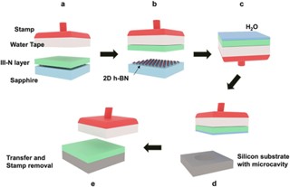
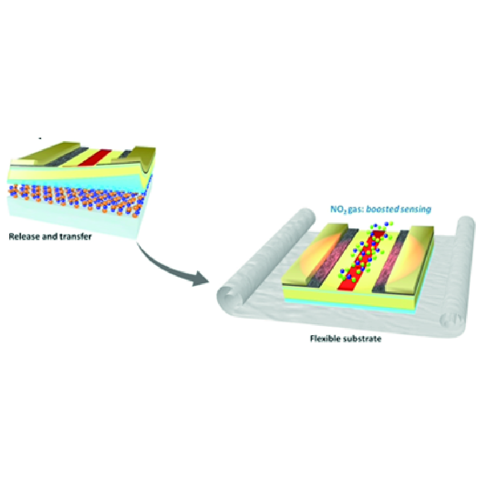
2D-assisted transfer technique
III-N Epitaxy by MOVPE
The most recent and significant developments in optoelectronics and electronics are mostly related to advances in the crystal growth of semiconductor heterostructures. The outcomes of these breakthroughs have been successfully demonstrated and have yielded understanding of the subjects beyond quantum phenomena. Furthermore, they have given rise to tremendous industrial growth and replaced several conventional systems.
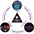
Photoinduced doping in hexagonal boron nitride for deep UVC application – BIRD project’s goals are to:
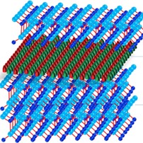
Reveal the underlying mechanism of insulator to conductor transition in 2D layered h-BN after deep UV illumination. The exact reason for giant PPC in h-BN is indeed still unknown hindering the development of the photoinduced doping effect. As such, identification of the defects responsible for PPC will be a fundamental input to favor their formation during metal organic chemical vapor deposition growth.
Optimize the giant PPC effect and effectively use it as a novel doping method. Understanding the physics behind the giant PPC effect in h-BN is a first requirement for that.
Demonstrate its proper usage we aim toward the realization of h-BN homojunctions using the photoinduced doping process to produce conductive h-BN layers. Integrating BAlN/BN quantum wells would then be the next step toward highly efficient DUV LEDs
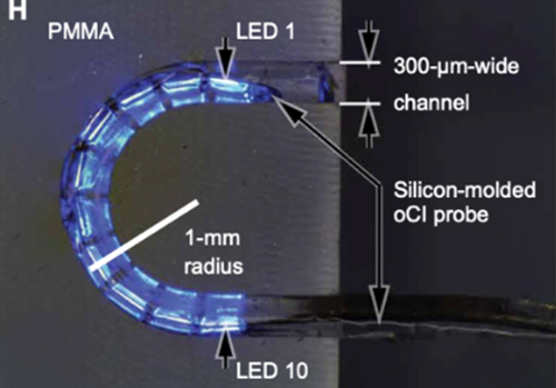
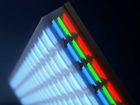
Due to the high electrical conductivity of cochlea tissue, optical nerve stimulation leads to better spatial resolution and more efficient implants. CORTIORGAN’s objective is to develop a specific manufacturing process to produce ultra-thin (< 5 microns) InGaN LEDs, 30 ?m x 60 ?m in size, which will be mechanically detached from a substrate and transferred to cochlear implants. The process is based on the growth of LED structures on h-BN/sapphire substrates, enabling us to meet the constraints of these new implants, which will be inserted into mouse cochleas at the end of the project.
Selective GaN growth on patterned hBN for transferring MEMS onto flexible substrates – FLEXIGAN
The FlexiGaN project aims at implementing and optimizing the selective growth of III-N layers and heterostructures onto pre-patterned hexagonal boron nitride (hBN) to fabricate high mechanical quality electromechanical systems (MEMS) that can subsequently be transferred onto flexible substrates.
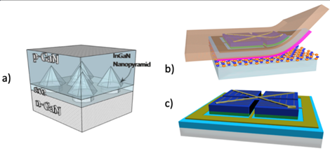
InGaN nano-pyramid-based Multi-terminal multi-junction Solar cells – INMoSt
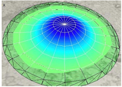
The purpose of INMoSt is the realization of low-cost, high-efficiency, multi-junction solar cells using a single material family, namely III-nitride semiconductors. This target becomes possible by combination of a series of innovative technologies. The first milestone will be the demonstration of beyond-state-of-the-art, free-standing, and flexible InGaN-based SCs. The ultimate goal will be the fabrication of a stack of such SCs, using a process fully compatible with conventional IC technology.
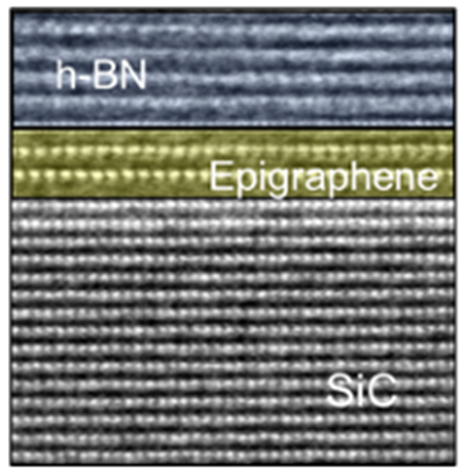
Films bidimensionnels épitaxiés BN/epigraphène/SiC pour la nanoélectronique – BONNEG
The aim of this project is to validate the operating principle of ultra-thin field-effect tunnel transistors based on two-dimensional graphene/boron nitride (BN) epitaxial heterostructures with a viable large-scale integration scheme. The first step is to produce very thin, homogeneous BN layers by deposition on epigraphene (epitaxial graphene on silicon carbide single crystal).
Dixit
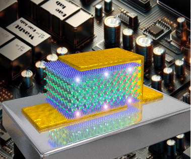
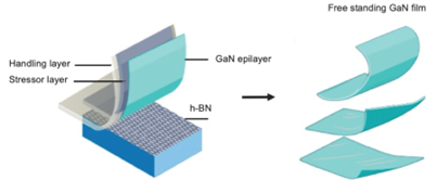
The development of power electronics devices using gallium nitride (GaN)-based materials continues apace. To date, GaN-based technologies are used in power electronics with horizontal field-effect transistors such as those with insulated gate on a specific heterostructure (MOS)HEMTs (High electron mobility transistor). However, due to their lateral operation, this architecture has two major drawbacks. The first is strong self-heating of the device, and the second is surface current leakage in the presence of a strong electric field. To avoid these drawbacks, new GaN-based vertical-structure transistors have been proposed in the literature. The DIXIT project proposes an approach based on the use of hBN/Al2O3 substrates for growing thick GaN layers and transferring them to metal substrates. The hBN layer greatly reduces the stress in the GaN layer, making it easy to detach and transfer to a host substrate. What’s more, the Al2O3 substrate can be reused without extensive recycling, thereby significantly reducing costs.
Biosensors
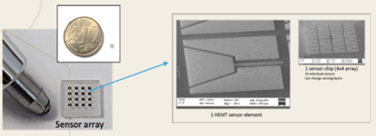
Today’s medical practices require considerable technological input to improve efficiency. The SARS-CoV-2 pandemic has highlighted the saturation of healthcare systems in France and abroad. This saturation actually existed long before the pandemic. There is a mismatch between upstream needs (primary care) and the lack of downstream resources (hospital beds). The aim of this project is to create a biosensor sensitive to biomarkers of interest and relevance to current medical practice.
Below is the list of our previous projects.
- Capteurs de gaz muLtifonctions pour anti-pollution A base de Nitrure de Gallium pour application automobile – CLEANING
- Convertisseur d’energie betavoltaiques a base de nitrure de gallium – BATGAN
- Nitrures iii-v deposes sur vErre pour un Watt PhotoVOltaique iNteGre a L’hAbitat baS cout et treS haut rendement – NewPVonGlass
- Epitaxie de composés semiconducteurs borés (III-B)-N pour applications en Hyperfréquence et optoelectronique – GABORE
